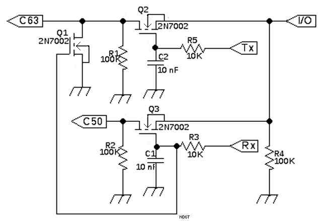
The BITX40 has always been plagued with a loud “pop” in the speaker when changing from transmit to receive modes or back again. This is especially annoying when wearing headphones and much more so when operating CW where it frequently switches. My builds have all had various ways of reducing that noise, the most successful by software control, but never as satisfactory as that solution suggested by Wayne Cheng, VA7AT. His fix was more complex, involving re-wiring the power to both the transmit and receive audio preamps and the gating the audio with MOSFETs.
I built a few boards and documented them here. Kees, K5BCQ, took notice and offered to provide full kits to the BITX community. As sales and kit stock declined, Kees terminated the project in early August 2018.
Although the circuit is designed for the µBITX it works quite well for the BITX40 as well. Not quite the click suppression, but far better than anything that I have tried so far. It doesn’t require special software, either, so you can use your favorite operating software. Even mine!
The kit is described in the µBITX pages of this site but since there are significant differences in the radios, and to avoid confusion, I will duplicate parts of the instructions here so that you don’t have to switch back-and-forth. Anything to make it easier, right?
This kit is shipped with all of the components, board, header pins, and foam tape attached to the schematic diagram with adhesive tape next to their parts listing. The surface mount components are in their sections of reel tape and secured by plastic film on the top. If the envelope has been roughly handled then some of these tiny parts may have escaped so when you open the envelope be careful to check for any components rattling around loose.
Remove the printed circuit board and place it in a small vise in a horizontal position. I recommend a vise as low to the work surface as possible. The higher it is placed, the more likely that part that escapes the work area will never be found. Lacking such a vise you can get by with a glob of “poster putty”. The dollar store variety is fine. Just stick a goodly wad on the work surface and embed the circuit board so that it is stable, secure, and flat.
I recommend a temperature controlled iron, 40 to 60 watts, with a small tip. I use .01” diameter solder for surface mount work since it provides superior control of solder quantity. Melt a small amount of solder on one of the pads for R3. Heat it just enough to melt the solder onto the pad but remove the heat before the flux cooks off. The idea is to leave enough for later re-flowing without additional flux.
Releasing the first bit of components at the top of the adhesive tape (two 10K resistors) you will find them attached to their original section of reel tape. Holding them close to the work surface (they bounce!) carefully remove the retaining film and tip them out. Use an ohmmeter to confirm their value and then place the first one in position on the pads for R3. Nudge it into place, centered as much as possible.
Hold the resistor gently in place with the end of a soldering aid, small tweezers, a stainless dental probe or some such, near the center of the part’s body. Apply the soldering tip to the joint at the pad that you previously prepared. When you see the solder melt hold the heat just long enough to give it time to flow onto the resistor and create a bond. Remove the heat and hold the part in place until the solder solidifies. Now pick up the solder and properly solder the other end of R3. Use just enough solder to make a nice fillet, ensuring a secure electrical and mechanical joint. Hold the hot tip on the joint long enough to cook off most of the flux but not so long that the other end of the resistor gets hot enough to melt the solder there and release the part to skate out of position. It’s a balancing act! More art than science. Now return to the first joint and properly solder it.
If the part skids out of place, use stainless steel tweezers to pick it up while alternately heating the connection(s). Use de-soldering braid to remove excess solder from the pads and then re-install. With practice you will develop the proper timing and you will seldom have a part slide out of position.
Next install R5, the remaining 10K resistor, using the same method. The three 100K resistors are to be installed next.
The three transistors are MOSFET and are sensitive to electrostatic discharge. Treat them accordingly.
With all ten parts mounted on the board it is time to prepare the BITX board for the kit. Remove C116 from the BITX and install it in the “C50” position on the kit board. This is a non-polarized ceramic capacitor. The new board is labeled in case you replace C116 with a polarized type. Do the same for C122, moving it to the “C63” position on the kit board , thus completing the component installation.
Now to re-arrange the preamp power:
Locate the TX bus trace near R127 in the main diagram. Cut it near where it is indicated on the sketch. Just remove enough to ensure that there will be no accidental connection. No need to scrape off any coatings at the cut but you do need to clean off the coating around the little via hole on that trace a short distance away that I have indicated with a “TX” and an arrow. This will be where the TX jumper will be installed later.
Quite near your cut is a via that goes to the emitter pin of Q16. Clean off that one for soldering also. That will be the location for the ground jumper.
Cut a jumper of small insulated hookup wire (like AWG 26 or so) about an inch long. Strip the ends about a 1/16” from each end and jumper from the 12 volt end of R101 to the end of R113 that connects to R111. Just solder right to the fillet at the ends of each resistor. A slightly shorter jumper should then be soldered from R111 to R127 the same way. This restores full time power to both amplifiers.
I will leave the option of using plugs and jacks to the individual. I prefer just hard wiring to keep things simple and avoid intermittent connections and to save space. At this point you can install the supplied header pins or just the six jumper wires to the board. Clean off any flux with alcohol or flux remover.
Instead of using the RX supply bus for steering the gating of Q1 and Q3 during transmit, timing issues force us to use the Push-To-Talk (PTT) line instead. The nearest access will be dependent upon the topology of your particular build. My nearest and easiest point was the microphone jack.
I mounted mine atop the components beside crystal number X5 using the foam tape. It is not an aggressive adhesive and releases easily if needed.
Check your work. Apply power. Enjoy the peace and quiet.de ND6T