The BITX40 has always been plagued with a loud “pop” in the speaker when changing from transmit to receive modes or back again. This is especially annoying when wearing headphones and much more so when operating CW where it frequently switches. My builds have all had various ways of reducing that noise, the most successful by software control, but never as satisfactory as that solution suggested by Wayne Cheng, VA7AT. His fix was more complex, involving re-wiring the power to both the transmit and receive audio preamps and the gating the audio with MOSFETs.
Although the circuit is designed for the µBITX it works quite well for the BITX40 as well. Not quite the click suppression of the µBITX , but far better than anything that I have tried so far. It doesn’t require special software, either, so you can use your favorite operating software. Even mine!
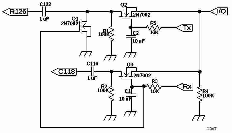
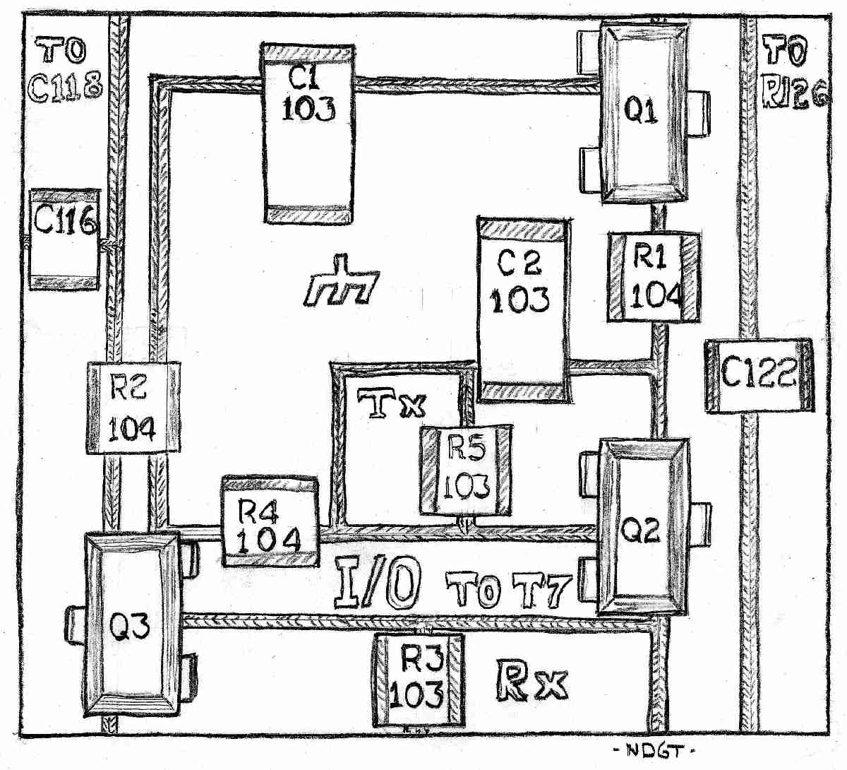
I used a piece of single-sided un-etched printed circuit board stock and arranged the parts on it to determine the width of the islands that were needed. I then used a hobby knife to cut channels to isolate the pads as shown in the accompanying drawing. I used a continuity checker to ensure that there was good isolation and then soldered the parts to the board. I removed C122 and C116 from the BITX40 circuit board (those 1 uF. blocking capacitors) and installed them on the new board as shown.
Not up to that much surface mount work? No problem! This is an audio circuit. Through-hole parts are fine. Make it as big as you want. Use perf-board or island construction. It really doesn't matter. Use 2N7000 or BS170 transistors. If you use polarized capacitors (like electrolytics or Tantalum) be sure to observe the correct polarity (positive end toward the BITX board, negative toward the drains of Q1,Q2, and Q3).
Now to re-arrange the preamp power:
Remove diode D18 or tombstone it so that that RX power to U1 is disabled.
Locate the TX bus trace near R127 in the main diagram. Cut it near where it is indicated on the sketch. Just remove enough to ensure that there will be no accidental connection. No need to scrape off any coatings at the cut but you do need to clean off the coating around the little via hole on that trace a short distance away that I have indicated with a “TX” and an arrow. This will be where the TX jumper will be installed later.
Quite near your cut is a via that goes to the emitter pin of Q16. Clean off that one for soldering also. That will be the location for the ground jumper.
Cut a jumper of small insulated hookup wire (like AWG 26 or so) about an inch long. Strip the ends about a 1/16” from each end and jumper from the 12 volt end of R101 to the end of R113 that connects to R111. Just solder right to the fillet at the ends of each resistor. A slightly shorter jumper should then be soldered from R111 to R127 the same way. This restores full time power to both amplifiers.
Instead of using the RX supply bus for steering the gating of Q1 and Q3 during transmit, timing issues force us to use the Push-To-Talk (PTT) line instead. The nearest access will be dependent upon the topology of your particular build. My nearest and easiest point was the microphone jack.
Prepare six wire jumper leads. Solder one end of each to the indicated pads on the new board.
I mounted mine atop the components beside crystal number X5 using foam tape. It is not an aggressive adhesive and releases easily if needed.
Check your work. Apply power. Enjoy the peace and quiet.de ND6T